Bitstuff

For people interested in how computers work bottom-up.

Friday, February 09, 2007

Subtract and Branch if Negative

I got pretty bored over winter break, and decided I needed a project to keep me busy until class started. Well, there was one thing that I've been wanting to do for a long time. I have wanted to build a simple computer out of 7400 series logic chips. I only had about a week for the whole project, so the design had to be pretty spartan. I also wanted to use chips that I had on hand, though that didn't last for too long.

After thinking up a few different ideas, I finally remembered another project that I've been wanting to do: build a Subtract and Branch if Negative computer. That is, a computer whose only instruction is to subtract two numbers, store the result, and branch to an alternative memory location if the result is negative. This is very much like SBN on wikipedia.

If you don't care to look at the Wikipedia page, the subtract and branch if negative instruction turns out to be the only instruction you need to build a turing-complete computer. That is, this one instruction, given enough time and memory, can compute anything that a regular computer can. Of course, it's slow, inefficient, and a pain to program.

So I went about designing a simple microcomputer based on this instruction. First step, I needed to decide on some basic specifications for the processor:

Data Width: 8-Bits
Address Space: 16-Bits
Instruction Set: Subtract and Branch if Negative

After that, I could rough out a block diagram of the dataflow. Using the dataflow as a guide, I figured out what chips I could use in what blocks, how many I would need and how they connect to each other.

The dataflow was the easy part. More difficult is designing the control logic, which was going to be especially complicated because of the 8 and 16 bit busses. This is because it now requires two cycles to read in the address of an operand, and another cycle to read in the value of the operand. This needs to be done once for both operands, and then again when we need to load the new PC value if the instruction takes the branch.

The control sequence for the processor goes something like this:
  1. Load MAR.H; PC++
  2. Load MAR.L; PC++
  3. Load B
  4. Load MAR.H; PC++
  5. Load MAR.L; PC++
  6. Load A
  7. Store ALU Result; PC++
  8. Load PC.L
  9. If (ALU Result is negative) {Load PC}
A pretty reasonable way to encode the control logic would be to program the control signals into an EEPROM. This is very simple and is easier to change if there is a bug. However, I had never used EEPROMs before, so I decided to build a state machine out of 7400 series logic. It's a bit of a mess, and there were a few bugs to squash, but it works.

So we have the control and the dataflow...what else? Input and output. There needs to be a way to load programs onto the device, and then a method of interacting with the running program.

I had initially thought about using a series of switches for loading programs into RAM. That was going to be incredibly tedious and time consuming, so I scratched that. Instead, I did some research on the Parallel port, and found it to be the perfect solution. It's easy to interface, easy to program and completely automated. This only required a few extra chips to interface the parallel port to the system bus on the microcomputer. Basically, it needs to be able to take control of the bus when it needs to program, and relinquish control when it's done.
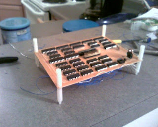
Last bit of hardware, the human machine interface. I have to admit, it's pretty craptacular on this microcomputer. An 8-bit dipswitch and an 8-LED bargraph are all the I/O you get. However, this fits in with the overall strategy of making somewhat rediculous design decisions. There is however, at least one neat trick that can be done to expand the output capabilities.

The fabrication of this computer is another story. I had hoped I would be able to build it on a printed circuit board, that would have been wonderful. However, I had too many chips for the free version of Eagle CAD I had. Simply would not fit on the board. So I decided to use a pre-drilled perferated board with solder pads. Good enough, but wiring ended up taking most of the week. Luckily for you, you don't have to wait to see the finished product. The final stage of the microcomputer has two boards. The bottom board has the processor, memory, power supply and clock generator. The top board holds the batteries, has some blinky lights, dip switch and some simple address decode logic for memory-mapped IO.

To wire up all the parts, I used a lot of wire-wrap wire, solder and a wire-wrap tool. The leads on the parts were very short, so wire-wrapping was a real pain, but it seemed to be the best way to get the leads into place for soldering. It was slow going and took about four very full days to finish. On top of that, I had to test and debug different parts as I finished them. It can make you pretty nervous when you have to desolder several connections on one IC to make a fix.
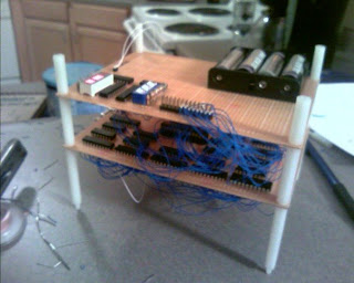
If I do another 7400 series-based microcomputer, I will get a proper wire-wrap board.

Now that the darn thing is built, what to do? The work's not done yet. After building and debugging it, I still needed to be able to write, assemble and load programs. I needed to write an assembler and program loader.

The program loader actually turned out to be the easiest part of the whole project. Programming the parallel port on Linux was much easier than I expected. In fact, the loader program only had one bug in it the first time I tried it. Made the fix, tried it again, worked!

Now that I could load any data I wanted into the microcomputer's memory, I needed an easier way to program it. This meant developing a simple two-pass assembler. On top of that, I wanted it to have some built-in pseudo operations, so I could program and still keep my sanity. Programming this device with only using the low-level subtract and branch if negative instruction is not my cup of tea.

Eventually I hacked out a simple assembler that fit the bill. The assembly code looks like this:

sub i, imm(-10)
loop:
dec i
bltz i, loop

This little snippet is a simple loop. It subtracts -10 from i (which it assumes to be 0), setting up the number of iterations. Each iteration it decrements the loop index, and continues to loop as long as "i" is greater than or equal to zero.

Each instruction in that snippet is a pseudo-operation that is converted into SBN instructions by the assembler. Furthermore, each of those pseudo-ops can be converted into exactly one SBN instruction.

The "imm(-10)" bit of code allows me to operate with immediate values in my code. All it does is return the address of the value"-10" on the constant table. These keeps me from having to allocate a memory location for each constant I use in my code.

I now have everything I need to write a demo program. I wanted the microcomputer to do something unexpected. Something you wouldn't think it would be able to do. I think the most limiting part of it is it's input and output. I decided the demo would be an output-only program. This leaves me with eight blinky lights to do something cool with.

So, the most unexpected thing to do, would be to project an image with those eight lights. That's my thought anyways. I was set on displaying a smiley face using just those lights. How, you might ask, can that be done? Using persistance of vision.

If you've ever looked at a flashlight in the dark, you've probably noticed that it seems to leave a trail when you look at it. If you spin it in a circle fast enough, you might see a circle of light, neato. The idea behind displaying a smiley face on the eight lights is the same. If I move the lights, or use a mirror to move them, your eyes will see a trail marking where that light has been in your field of vision. If we setup a regular motion of a mirror, and display one line of the image at a time, we can display an entire 2D image using one line of eight lights.

So that's what I did. The program outputs one line of the desired image, blanks the lights for a split second, the next line is lit up, and so on. I took a picture of the effect with my camera. I don't have any mirrors yet, so I just panned the camera across the lights in the dark, it worked out really well. To show other people, I can just shake the lights up and down. Eventually, I would like to get a small mirror, motor and switch for synchronization. That seems a bit safer than shaking the fragile computer.

In the end what I got is an 8-Bit computer with one instruction, 32 KB of RAM and a clock speed of 250KHz. Though it takes nine cycles to execute one instruction, so in reality, it's executing about 28,000 instructions per second.

Sunday, May 28, 2006

Epiphany

So I just realized that a multiple-issue superscalar processor is not at all efficient in an fpga. It simply will not provide the performance I'd like for one major reason: multiple write ports in FPGAs are prohibitively expensive.

So what I will do, is create a one-issue out of order processor that runs at a very high clock rate. The goal is 200MHz. We'll see. The scheduling hardware will be much cheaper this way. Also, it will be faster than a slower multiple-issue processor on an fpga.

Basically, my one choice for implementing multiple-write ports was to time-multiplex the register files. This creates some asynchronous fun. I figured as long as I was doing the time-multiplexing for the register files, I might as well time-multiplex the write back bus. Turns out, that is not such a bad idea. In fact, I should make things easy and run everything at the higher clock speed and pipeline where I have to. This would make a 200MHz scalar out of order cpu similiar to a 50MHz four-issue cpu. Tada! But it's even better, because many instructions will take only one cycle, while others, like addition, will take a couple.

Neato, right?

Tuesday, May 09, 2006

CPU Project Calendar (sortof)

Looking at this whole project at once is a bit intimidating, so I split it up into a few different stages.

  1. Overall Architecture
    1. Concrete design parameters
    2. Number of functional units and their partitioning
    3. Major units
    4. Busses between units
    5. ISA (likely to be a subset of the M-word)
    6. Scheduling algorithm
    7. Do some quantitative analysis to back up design choices
    8. At this point, I should have a bunch of nifty drawings and all-around fuzzy feelings about the project
  2. Basic Processor
    1. Implement instruction decode for basic arithmetic instructions
    2. Implement 4-issue scheduling hardware
      1. Dependency FIFOs
      2. Register file
      3. Re-Order Buffer
      4. Write-Back bus arbitrator
    3. Implement basic ALU functional units
    4. Bypass hardware
    5. Instruction memory (trivial)
    6. Trackers, trackers, and more trackers
      1. Make sure to have good debugging information
      2. Possibly implment a transaction checker
    7. At this point, I should have a good testbench environment and be able to calculate the fibbonacci sequence along with some other basic programs
  3. Branches
    1. Implement branch functional unit
      1. branch
      2. jump
      3. trap
    2. Implement branch prediction unit
      1. Branch prediction table
      2. Branch target buffer
      3. Return address stack
    3. Implement branch-misprediction rollback mechanism (should be trivial)
  4. Load/Store + Cache
    1. Implement Load/store functional unit
    2. Implement data and instruction caches
    3. Implement bus interface
    4. Implement cache system instructions
  5. TLB + interrupts/exceptions + Finish implementing all instructions
    1. TLB
    2. interrupts/exceptions
    3. finish all instructions
  6. Floating Point Units?
    1. This would be nifty. We'll see how much space is left.
  7. At this point, I should have a working processor. Pat self on back.

Thursday, May 04, 2006

x86 ISA

I kindof think it would be cool to implement a 80386-compatible CPU. It would be more relavent to my interests, even though the ISA isn't nearly as clean as a RISC CPU. Funny thing is, I've only been designing RISC CPUs, so maybe I should take a detour to the dark side of CISC anyways.

I think I will still piece together the requirements and solutions for the superscalar processor; but in the interim, I want to hack together an x86 CPU.

Fun stuff.

Tuesday, May 02, 2006

HOT16 ISA

I thought I'd post the ISA encoding of the "speed-demon" processor I created. It really did have a ridiculously high-clock rate for being implemented in an FPGA. It also was quite efficient with resources. It is a dual-issue statically scheduled processor. The two issue slots have their register file, registers from the other file are accessed through a few instructions. Operands from the other register file are denoted by a preceding "x.".

The major problem with this processor is that it is a super pain in the bum to program. I didn't even bother, because I knew it would vaporize my brain if I tried. It's only a 16-bit processor with 16-bit addressing. It has a carry flag and add with carry to facilitate adding larger numbers. It has several shift operations to implement a fast multi-cycle barrel-shifter of sorts. There are one to three delay slots after each instruction depending on how much forwarding logic is included when the CPU is instantiated. The forwarding logic costs cycle time, but I'm not sure this processor would be possible to efficiently schedule with 3 delay slots before the result of an instruction can be used, especially with only 8 registers per issue slot.

So even though it has all these shortcomings, I did some quantitative analysis to see how fast it is compared to another 32-Bit Pipelined RISC processor I designed. Turns out, with perfect instruction scheduling, the processor is 5 to 10 times faster than the 32 bit processor, leaning towards the lower-end with more 32-bit instructions. With more realistic scheduling, say, one instruction per cycle on average, it is still 2 to 5 times faster. Along with the fact that 12 of these can fit on a chip, it could actually get some pretty decent performance. Definately not general-purpose computing, however. It is more akin to the cell architecture with attached processing units.

Instruction

Type

[15:14]

[13:11]

[10:8]

[7:3]

[2:0]

ld rt, imm8(rs1)

Rm

10

rs1

rt

imm8

st rt, imm8(rs1)

Rm

11

rs1

rt

imm8

addi rs1, imm8

I

01

rs1

000

imm8

subi rs1, imm8

I

01

rs1

001

imm8

cmpi rs1, imm8

I

01

rs1

010

imm8

andi rs1, imm8

I

01

rs1

011

imm8

lui rs1, imm8

I

01

rs1

100

imm8

b.cc imm8

I

01

n

z

o

101

imm8

jr rs1

J

01

rs1

110

00000000

jal imm11

J

01

imm11

111

imm11

add rt, x.rs1, rs2

R

00

rs1

rt

00000

rs2

sub rt, x.rs1, rs2

R

00

rs1

rt

00001

rs2

or rt, x.rs1, rs2

R

00

rs1

rt

00010

rs2

and rt, x.rs1, rs2

R

00

rs1

rt

00011

rs2

add rt, rs1, rs2

R

00

rs1

rt

00100

rs2

sub rt, rs1, rs2

R

00

rs1

rt

00101

rs2

or rt, rs1, rs2

R

00

rs1

rt

00110

rs2

and rt, rs1, rs2

R

00

rs1

rt

00111

rs2

addc rt, rs1, rs2

R

00

rs1

rt

01000

rs2

xor rt, rs1, rs2

R

00

rs1

rt

01001

rs2

not rt, rs1

R

00

rs1

rt

01010

rs2

mulhi rt, rs1, rs2

R

00

rs1

rt

01011

rs2

mullo rt, rs1, rs2

R

00

rs1

rt

01100

rs2

sll.m rt, rs1, imm3

R

00

rs1

rt

0111m

imm3

srl.m rt, rs1, imm3

R

00

rs1

rt

1000m

imm3

sra.m rt, rs1, imm3

R

00

rs1

rt

1001m

imm3

sllv.m rt, rs1, rs2

R

00

rs1

rt

1010m

rs2

srlv.m rt, rs1, rs2

R

00

rs1

rt

1011m

rs2

srav.m rt, rs1, rs2

R

00

rs1

rt

1100m

rs2

test rs1

R

00

rs1

000

11010

000

RESERVED

R

00


11011


m: [L=shift 0,1,2,3 bits | H= shift 0,4,8,12 bits]

Monday, May 01, 2006

A Complexity-Effective Dynamic Scheduling Algorithm

I found this paper online:

http://courses.ece.uiuc.edu/ece512/Papers/Palacharla.1997.ISCA.pdf

This method uses register renaming along with dependency checking in instruction dispatch to reduce complexity in the wakeup-select logic (reservation stations). A FIFO is setup for each issue slot, instructions are issued to FIFOs so that dependency chains are located in FIFOs. This means that instructions only need to be checked at the head of the FIFO if they are ready to be dispatched to a function unit.

This could greatly reduce the cycle-time and resources used by the scheduler in an FPGA CPU.

New Reservation Station Operand Design

A couple things I can do to optimize the size of reservation stations.
  • Don't store data in the reservation station itself. Instead, store only the tag of the operand. This saves a ton of luts and flipflops because multiplexers are expensive in FPGAs, and without the data, we significantly reduce the width of the multiplexer required. We also don't need a multiplexer from each of the write-back busses because we don't need to save the data. Data for outstanding tags can be stored in a special register-file because register files can be implemented as distributed RAM. This basically combines the storage and multiplexer into one relatively tiny alternative. The drawback is that the in-flight register file will need two read ports for each functional unit and one write port for each write-back bus (there are some time-multiplexing tricks to alleviate this issue). This should still be cheaper.
  • Something like 90% of instructions have only one or none of their operands outstanding. Therefore, most reservation stations only need to compare one operand at a time. This allows us to save a bit on comparators (which are relatively cheap in the Spartan 3 fabric).
The utilization savings are huge:
  • 7 slices VS 82 slices
  • 6 flipflops VS 39 flipflops
  • 10 LUTs VS 200 LUTs
Something like 10 times smaller. Also somewhat faster (~200MHz). Hopefully this is correct and will work out.

Dynamic Instruction Scheduling Algorithms

For my latest processor design, I want to do a modern processor design. This can mean many things. To me, it means it must have the following qualities:
  • Out of Order Execution
  • Speculative Execution
  • Superscalar
  • At least L1 Cache
  • Memory Management Unit
The most expensive quality is Out of Order Execution. I had read a paper on OOO using the Tomasulo Algorithm. Really quite helpful. However, the reservation stations are far too expensive to implement. A dual-issue superscalar CPU with out of order execution would require something like a 32 entry Reorder Buffer to be efficient. This would then require 32 reservation stations to hold instructions waiting for their operands to become available. Each reservation station requires at least two slots to compare operand tags and hold operand data, each operand slot requires one tag comparator for each write-back bus. This is waaaay to much resources for the FPGA I have. In fact, it uses > 100% resources on the chip :/

So now I'm researching other alternatives. I would really like to be able to do a four-issue processor, however, I don't think it's possible at this point.

Here are some resources I'm currently reading:
  • http://courses.ece.uiuc.edu/ece512/Papers/sched.html
  • http://www.cs.swan.ac.uk/~csandy/cs-323/09_dynamic_scheduling.html
  • http://courses.ece.uiuc.edu/ece512/Papers/Dwyer.1992.MICRO.pdf
Pizza out.

Sunday, April 30, 2006

Hello

I started up this blog to post updates on the various projects I undertake. I enjoy designing and implementing CPU designs and the like. People who truly enjoy something like that are far and few inbetween. Hopefully I can provide some interesting content to people and even get some feedback on the stuff I work on.

I learned synchronous digital design not quite a year ago. Ever since I've been focusing on implementing my own computer system and porting Linux. I've created several different processors in this time. Most of them are based on the MIPS instruction set, two of them weren't. Of the two that differed, one was a Subtract and Branch if Negative machine. Very slow, but with enough time, just as capable as any other cpu.

The other was a 16-Bit dual issue superscalar processor I designed specifically for a high clock speed on an FPGA. I was able to sanely fit 9 of these processor cores in one Spartan 3 FPGA. Theoretically it should be very fast, however it's programming model is a major pain in the bum. One core alone would operate at 180MHz on an FPGA. The nine core version operated at about 150MHz.

So now I'm trying to figure out the most cost-effective/performance cpu design, for the FPGA development board I have, that can run Linux. Then I will port Linux to the board, say "Woop-de-doo", and pat myself on the back for a job well done.